* Update murata naming to Murata

fix
- Converter_DCDC
- Crystal
- Inductor_THT

* Update file names to 'Murata'.

Initial commit did not include renaming
of the file names directly. This is now fixed

* Include changes suggested in PR at https://github.com/KiCad/kicad-footprints/pull/1681#issuecomment-694798043

* Fix Resonator_SMD_Murata_SFECV-3Pin_6.9x2.9mm_HandSoldering

* Fix Resonator_SMD_Murata_SFSKA-3Pin_7.9x3.8mm_HandSoldering

* Fix Resonator_SMD_Murata_TPSKA-3Pin_7.9x3.8mm_HandSoldering
* Fixed wrong Y pin spacing of Choke_Schaffner_RN202
Y pin spacing before was 10mm and has been fixed to 15.2mm.
* Fixed missing pads required for XP Power ITQ series
Current footprint Converter_DCDC_XP_POWER-ITxxxxxS_THT is incompatible for linked XP Power ITQXXXXS(A) series as pins 5 and 8 are missing. For ITQXXXSA (single output) series these pins are not used but physically there while for ITQXXXXS (dual output) series pin 8 is required for negative output voltage.
Changes:
1. Added missing pads for pin 5 and 8
2. Updated the link of both ITX and ITQ series datasheets
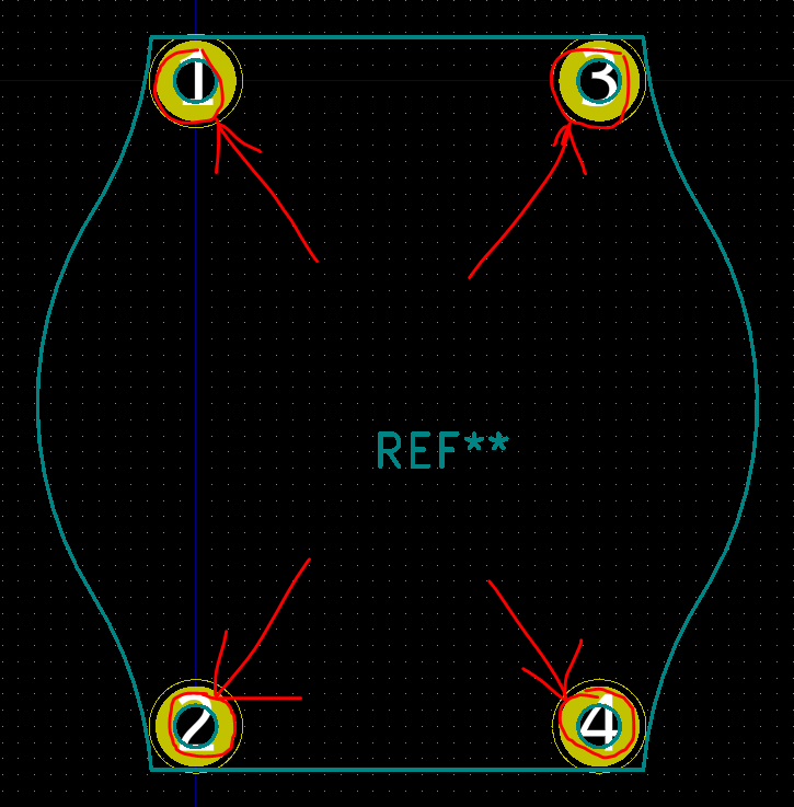
* fixed wrong pad to silkscreen Y offset
I see the problem, I only added 1 time the 0.11mm....
Updated the drawing, this is the original (F.FAB):
And 0.11mm larger for F.SilkS:
resulting in:
- [X] All symbols in Device.lib are generic so the pinout can vary or there can be multiple versions with different pinouts. However, the symbol you're showing above is outdated because it doesn't exist in the HEAD commit at https://github.com/KiCad/kicad-symbols/blob/master/Device.lib. So, if the dots on this component should be on pins 2 and 3 (or 1 and 4) using the datasheet, we can submit a new symbol with a different pinout to match. Since I'm not familiar with the convention given in the datasheet, if we can figure it out then we can match the datasheet pinout on the footprint too which I think is best. You?
--> The generic symbol with the dots is the only way of drawing a common-mode choke, in which the dots represent the input side of the filter. Because this filter contains only 2 coupled coils (I think therefore that this is the reason for the U-shape in the middle of the symbol in the datasheet) it is irrelevant which side is used as input.
I agree that it would be best to match the footprint with the pinout in the datasheet, but this would mean to create also a new symbol?
- [X] While the part is electrically fine using the EMI_Filter_CommonMode symbol (windings from pins 1-2 and 3-4), can you adjust your pin number locations to match the datasheet? Putting pin 1 at lower left will make this a bit more clear and avoid any questions later.
- [X] Place the silk ref des outside the part body. You can move the fab value inside the part body, if you like, since this part is big enough to hold it inside.
- [X] The horizontal courtyard lines need just a small tweak. The horizontal (top and bottom) fab lines have X locations of -1.5mm and 14mm. The courtyard should therefore be -1.75mm and 14.25mm, but yours are just a bit small. Can you push those out just a hair?

Regarding the pin numbering, I think we have to leave the data-sheet when it comes to pin 3 and 4:

So I would say to stick to the EMI_Filter_CMode and place pin 3 and 4 on the same location (which I already did in this commit)?
--> I was already wondering from which standard these dimensions where from, I downloaded a doc about the IPC levels. I adjusted the holes back to 1.2 and 1.75mm. I aumed based on your last comment that you found them too small that's why I enlarged them.
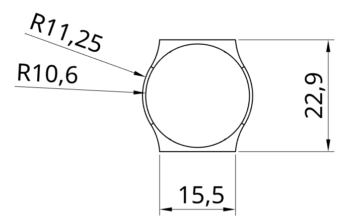
The part is now 1mm taller than the max in the datasheet, but the width is about exactly what the datasheet says. Can you balance that? And I just noticed the datasheet marks overall height and width as "max" so really it could just be +/-0.1mm oversize since they aren't nominal. My mistake. So if the height is 22.9 and width is 22.5 I think that should be good.
--> I changed the dimensions to the values you mentioned, and I updated the width on bottom and top to 15.5mm.
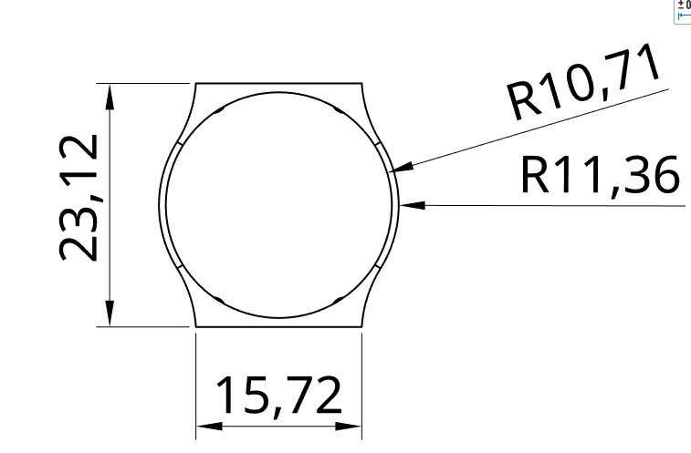
Courtyard should be 0.25mm outside of the fab lines, so it's a bit oversized now.
--> Yes indeed, I think I made a mistake last time.
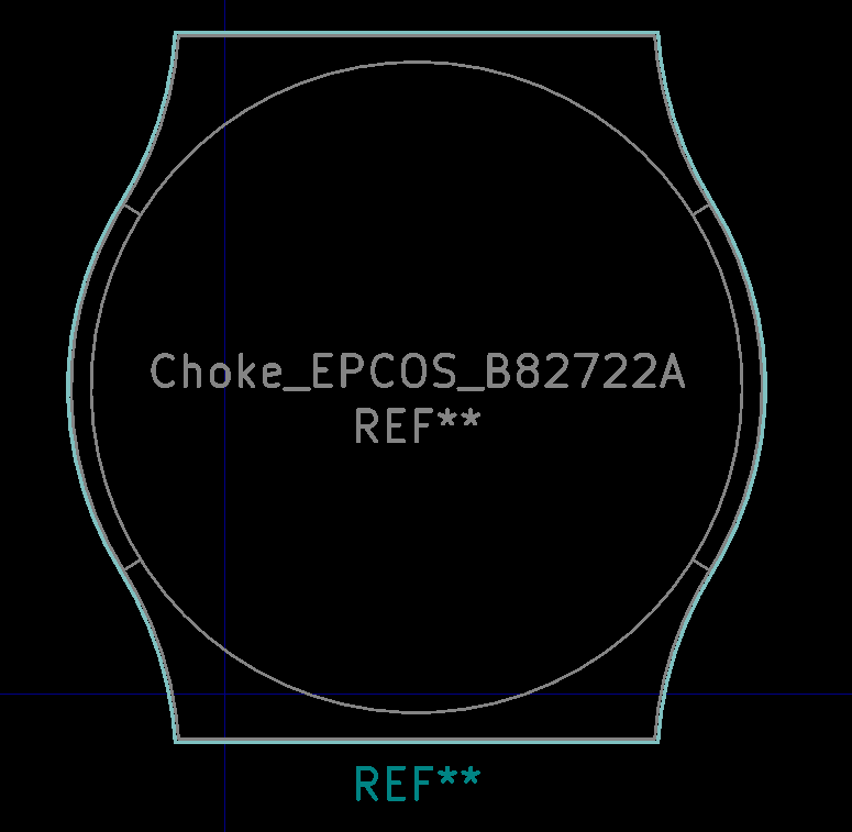
The inner circle is composed of 6 arcs. It would be simpler and preferable to use a single circle.
--> removed 5 arcs and changed 1 to 360 degrees.
You changed the corners to a curve, but I'm not so sure about that. I see pictures online all look like some kind of curve, but the datasheet shows square ends. Do we know that there aren't multiple plastic injection suppliers and the part can come with square instead of rounded ends? Maybe the drawing is just lazy? I don't know but since the datasheet hints at square corners making our footprint support square corners seems appropriately conservative to me. What do you think?
--> I agree with the square corners, they make it more dimensionable than the round ones and indeed the datasheets hints on square ones. The round ones were derived from the 3D model in which they ended up in the dxf file.
--> I increased the width and height by 2 times 0.5mm.
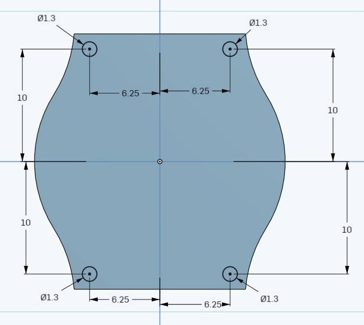
-->The holes are increased to 1.3mm and the pads to 2.6mm.
- [X] Courtyard cannot be curved because of issues with unclosed shapes.
- [X ] Fab lines are actual size and silk lines are outside the part body.
- [X] Pin 1 placed for footprints is specified at http://kicad-pcb.org/libraries/klc/F4.2/. That generic symbol could go with any footprint which may have very different geometry even with pin 1 always top left.
Yes, in some way Farnell has: [http://www.farnell.com/datasheets/1860373.pdf?_ga=2.15642422.1600121449.1528266424-1651149783.1519657816](url)
- [X] How did you draw this? The datasheet doesn't exactly show the curves so I'm wondering how close it actually matches the real part. --> I've drawn the symbol online in 3D at onshape.com(I do have FreeCad now so next time I will use that and try also to create KiCad 3D shape).
The curves are pragmatically determined as they have to intersect at the corners.
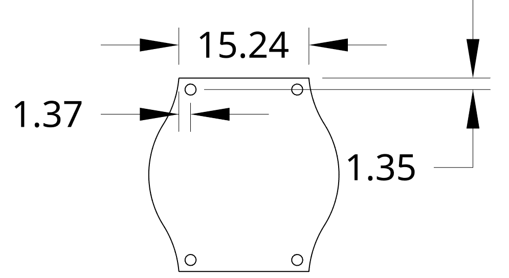
The horizontal distance of 15.24mm is measured from a real part:

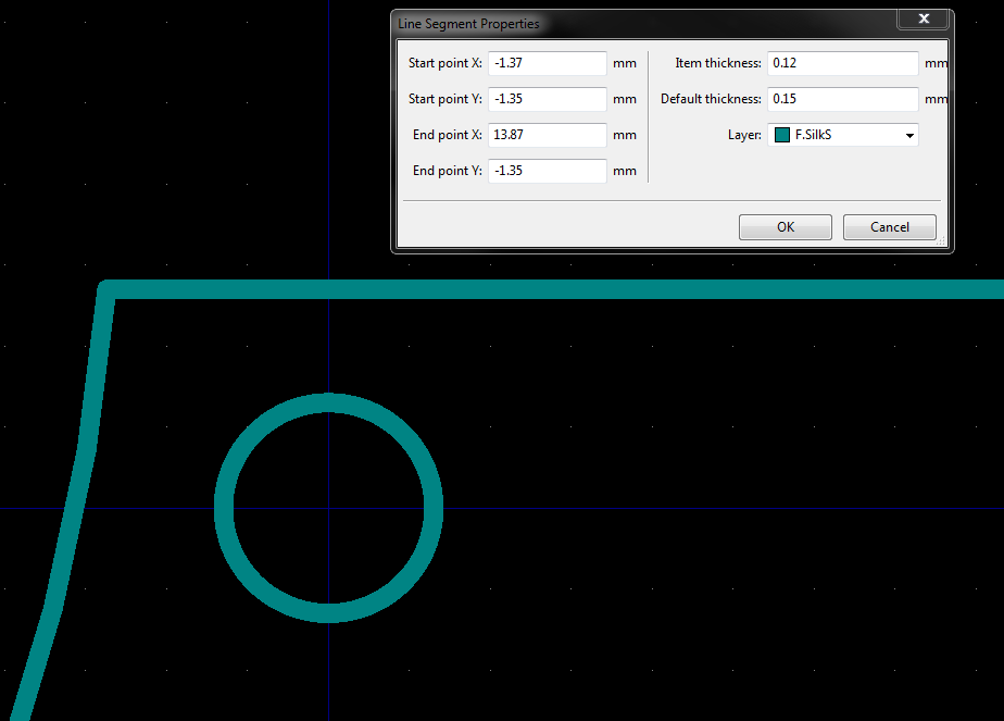
After import to the silkscreen I've used the pin indication to align the drawing with the pins on the TOP/BOTTOM layer in KiCad. I have done this at 0.05mm grid.
After this I checked the offset and moved the whole imported dxf drawing via the exactly move option to get it placed on whole numbers and compared it to the dimensions from the 3D-drawing:
Next i removed the pin circle's from the silkscreen.
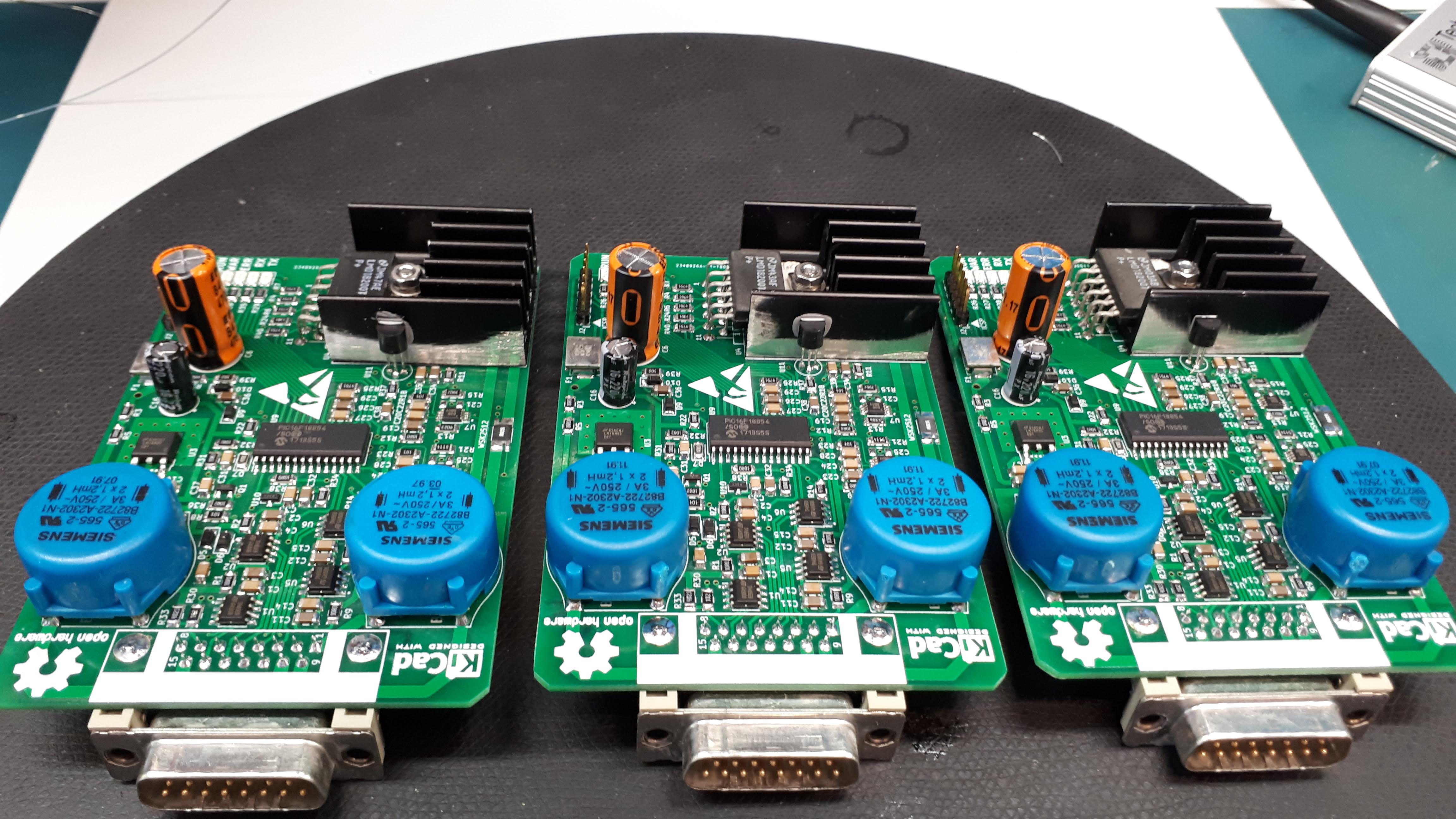
Proto's build with this component:
As you can see these (older ones) are from Siemens but have the same number.
- [X] From https://www.digikey.com/catalog/en/partgroup/b82722/5128?mpart=B82722A2302N001&vendor=495 it appears that B82722A is the rounded part in the datasheet and B82722J is the rectangular one. So this footprint could be called just Choke_EPCOS_B82722A. Please check me --> yes true, the ones I have here I found at Farnell at number 1223076. But the name Choke_EPCOS_B82722A is correct I will change the name.
- [ ] Courtyard should be 0.25mm from the copper or part body. We can make an allowance here because the shape is odd but please hit this dimensions on the top, bottom, and both sides. --> If allowed also to have arcs in the courtyard I can easily do it by drawing a 3d-shape 0.25mm bigger and export it also to dxf etc. Or only the horizontal and vertical lines have to apply to this? I would prefer import because it looks nicer.
- [X] Fab lines should be 0.1mm thick.
- [X] Silk lines should be 0.12mm thick.
- [ ] Silk lines should be offset form fab lines by 0.11mm. --> I assume the silk lines are the actual size of the component where the fab lines are smaller by 0.11mm or the other way around?
- [X] Pin 1 should be located at the top left.--> done, although it feels strange compared with the default symbol EMI_Filter_CMode
- [X] The dimensions are not at all close to round numbers which makes it a bit hard to check if everything is exact. It's a few tenths of a mm too narrow and it's just about 0.01mm too high. Can you make the numbers more round so it's easier to check and verify?