The notes also have some pictures of the test boards (I don't have the
current design in hand yet) to give some idea of what the heck this is
if you don't read KiCad files.

Signed-off-by: Linus Torvalds <torvalds@linux-foundation.org>
8.4 KiB
Notes on signal passthrough
Background
My older pedal designs all did "true bypass" with the stomp switch acting as a physical switch for the signal, so that when the pedal was inactive the signal would just pass through the pedal without ever going through any other component.
That obviously worked fine, but was really boring from a circuit standpoint. So out with that simply physical switch, and in with a electronically buffered pedal. Lots of commercial pedals do that, so it can't be entirely wrong.
You can do buffering multiple ways: using an actual analog switch IC, or typically using a JFET or a pair of MOSFETs as a switch.
Or even just not switching the signal at all, and instead just making the actual pedal circuit have a "neutral" mode where it doesn't affect the signal that is either triggered by the stomp switch or is just a fundamental part of the pedal itself (eg a pure buffer pedal possibly with just a volume knob and no stomp switch at all).
In a digital effect, a neutral mode might be done as a passthrough mode on the codec chip, or by just having a "NULL effect" on the digital side. The latter is in fact the only mode that the Daisy Seed board implements (possibly because the PCM3060 codec chip it uses doesn't even support it, or maybe due to the PCM3060 is hooked up in "HW mode" and so the controls aren't exposed).
In my very limited testing of the Daisy Seed, a clean passthrough through the ADC and DAC looked fine, but added roughly 5.2ms of latency to the signal. I suspect an actual musician can "feel" that, but my limited "make horrible noises on a guitar to see" certainly didn't.
But I can most definitely see it on the oscilloscope, and it just feels wrong. So I'm doing "proper" electronic switching.
Implementation
The bypass path is the dual JFET LS844 used as a high-impedance buffer, with the signal then going to the effect for processing. At the output, a control signal then picks either the original buffered signal or the processed output using a few MOSFETs.
A single MOSFET is already a switch, but the inherent body diode means that it always passes current in one direction. Putting two of them in series with the body diodes in opposite directions solves that issue. So to switch two signals you need four MOSFETs.
I'm using two dual complementary MOSFET packages that each contain one P-channel and one N-channel MOSFET transistor, which means that I can use a single control signal for them all to switch one set on, while the complementary transistors get switched off.
So the signal path always goes through the JFET buffer, then either goes to the effect board or not, but regardless of the path at the end the signal passes through the MOSFET switch that picks one or the other.
Additionally, it gets biased to ground at the start and the end, and for the MOSFET switching it gets biased to half the power rail so that the control signal (at ground or at +9V) is emphatically outside the signal range.
"Pretty" pictures
This is roughly how the jacks board looks. I say "roughly", because these are actually two different revision of the earlier test boards:
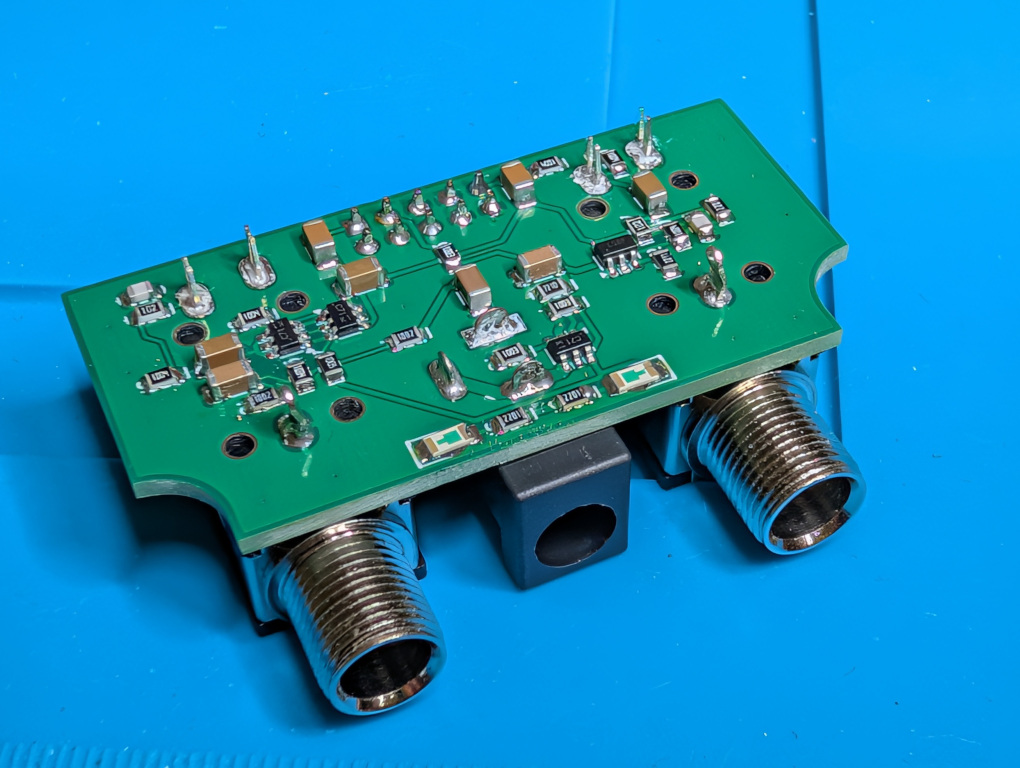

but while I've moved things around and modified the board layout (and outline) a bit, the circuit has stayed mostly the same. The following oscilloscope screenshots were taken with that "Component side" board (the "Connector side" is a picture of just the connectors placed on an unsoldered board with a more recent layout).
Results
It's not quite as clean as true bypass, and I wish my measurement environment was cleaner. The basic noise level for my signal measurement looks to be at around half a millivolt P-P, and I'll just blame cabling, environmental noise, and just plain incompetence with a signal generator and oscilloscope.
My el-cheapo signal generator also seems to have a slight DC bias, although it's also worth noting that some of the screenshots are with an extra bias just to have the waveforms not overlap 100%. Because many of them are that good.
Let's start with the not-great part: the noise. This is the oscilloscope screenshot of a 0Hz signal from my signal generator, with a vertical scale of 1mV per division and both channels limited to a 20MHz bandwidth:

on the screenshots the input signal is on channel 2 in cyan, with the output on channel 1 in yellow. You can see that the noise band on the output is bigger than on the input, but it's all high-frequency noise, and it's not horrible. The measurements say 4mV+ PtP. Not great, but none of it is audible.
I can clean a lot of it up with more aggressive low-pass filters, but for now I've only done some very basic RF filtering on it all.
Anyway, with that out of the way, let's look at the better part of the story.
I'm using a triangle wave for testing, because that visualizes non-linearities well - it's much harder to judge how good a pure sine wave is - and tends to also show any frequency issues.
Basic 1kHz signal, 1V peak-to-peak:
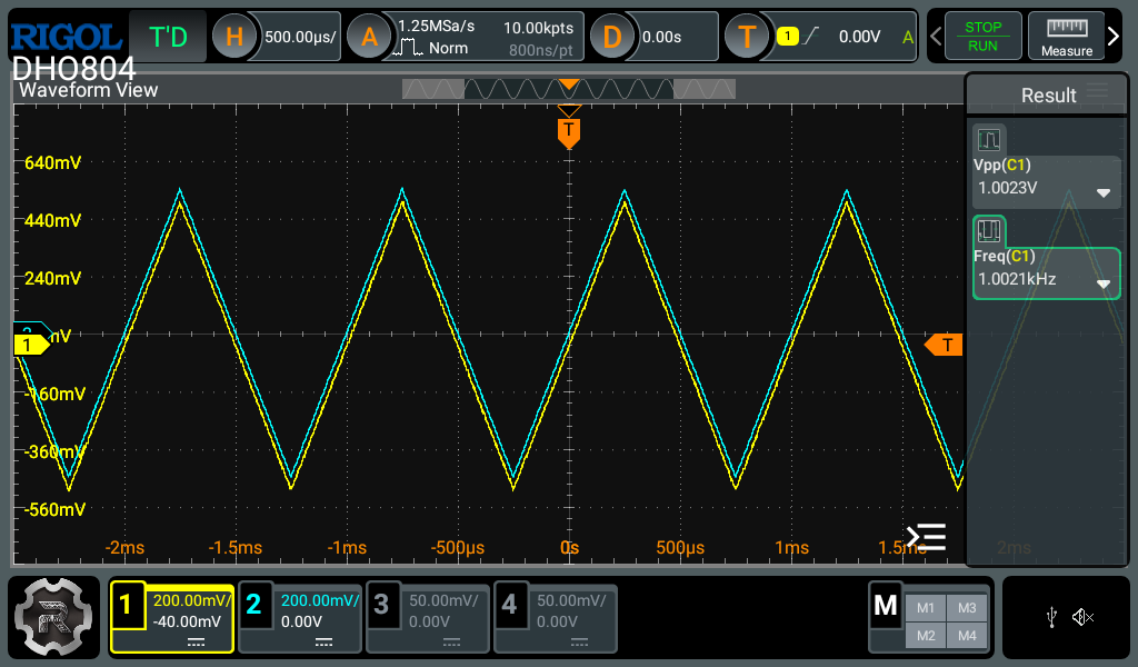
note the -40mV bias on the output signal - without that you don't see two signals at all because they overlap pretty much perfectly. The oscilloscope says "1.0023V" peak-to-peak measurement, but that's literally just from the noise. It's basically perfect.
Staying at 1kHz, this shows a 2mV PtP signal input just to show how the noise looks on a small signal that is in the same ballpark:

so it's still clearly a triangle wave at the output, despite the noise.
A more realistic signal level for guitar might be 200mV PtP, still at 1kHz but now artificially made worse by disabling the 20MHz bandwidth limit on the oscilloscope:

So it does ok on that 1kHz signal in the sub-1V range. What about other cases?
Here's a stress-test: 6V PtP with a 9V supply, still at 1kHz:

note the -200mV offset on channel 1, because without that it would still basically look like a single signal. There's a slight dip on the peak, but honestly, it looks quite good to me. So let's take a look at where it really starts failing.

Ok, it's most definitely not rail-to-rail in 9V, but I think I've seen real op-amps that do worse than this. That's obviously a very rounded top of the waveform, but a 9V signal is not realistic and I'll take this as a decisive win.
Going back to a more relevant worst-case 6V PtP signal (ok, still not at all realistic, but since it looks find, why not?, here's the 20kHz signal:

and you can see the same slight rounding of the top of the signal and it has maybe lost a tiny bit of sharpness of the triangle wave, but keep in mind that a 20kHz triangle wave has a lot of higher-frequency harmonics, so that's part of it.
How high will it go? At 100kHz, the RF filtering is starting to really show some attenuation of the higher harmonics, and you see more rounded peaks and it's not looking like a sharp peak any more. But remember: this is 100kHz, just checking the circuit, not relevant for audio:

The above basically tells me that I need to do a lot more high-frequency filtering, but for checking that the signal path is at least able to comfortably handle any signal in the audio range, it looks good.
Going the other way is more relevant, because bass frequencies can get filtered out by bad AC coupling. So here's that same 6V PtP but at 20Hz:

Still looks linear with straight lines and no sagging.
Anyway, if anything, I will need to add more low-pass filtering: the RF filters that the jacks have will filter out radio noise, but clearly it wouldn't hurt to be much more aggressive to get rid of power supply noise etc.
It's also worth noting that these screenshots were taken without any actual effect board connected. In past experiments, the Daisy Seed output has been very noisy indeed and it needs a lot of filtering to look good on an oscilloscope. So this is all the baseline performance just from the core input buffer and the output switching.