Altium Library Demo
This repository demonstrates the ability to view .schlib symbol files and .pcblib PCB footprint files using AllSpice.

Overview
AllSpice provides a platform for hardware engineers to collaborate on electronics design, much like GitHub but tailored for hardware projects. This repository showcases how to handle schematic library (.schlib) and PCB library (.pcblib) files within the AllSpice ecosystem.
Features
- View
.schlibsymbol files directly within the AllSpice interface. - Examine
.pcblibPCB layout files without needing external tools. - Track changes and collaborate on hardware designs using AllSpice's version control capabilities.
- Visual diff of symbol and layout changes
- Attribute Diffs
- AllSpice Actions can be used to verify your components
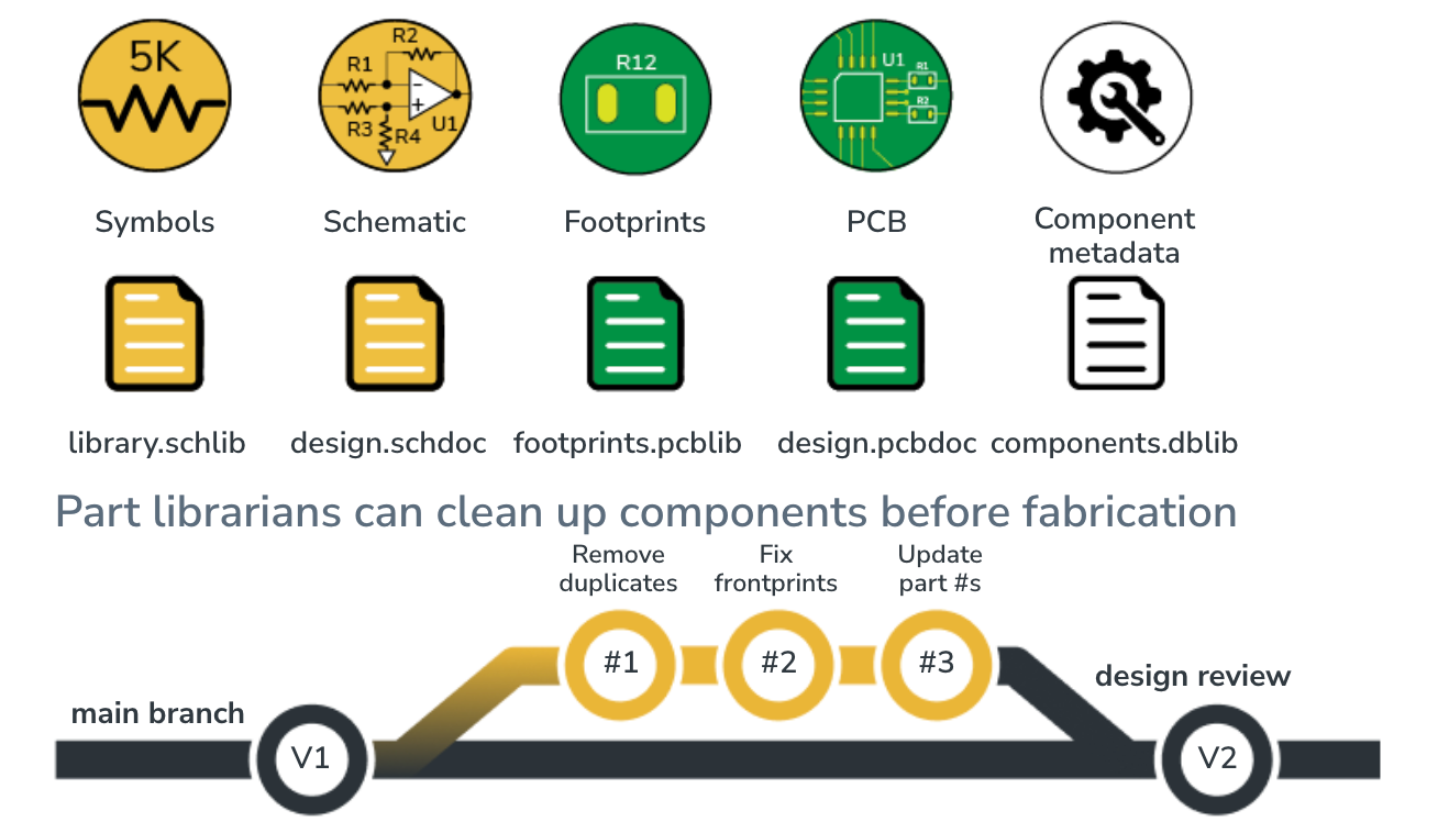
How does library management work?
Every component library starts with a set of project files.
Create a component library repository
Create a location for your designs. This can be as sophisticated as a git repo, or a shared network folder.
Discuss the location and logistics with your team before implementing. The most important thing is that everyone will reference the centralized library instead of creating their own.
Separate symbol and component files by function
Separate components into separate files by function. Each one of these component types have different common attributes and are easier to maintain and fix.
- Resistors
- Capacitors
- Connectors
- Power regulation
- Level translators
- High speed digital
- Radio frequency
Sometimes it’s easier to understand an example. Check out one of these library examples to see how we separate components.
Pair symbol libraries with footprint libraries
Ensure that symbol libraries and footprint libraries have synchronized names and known folder locations. If the libraries get separated, they have a tendency to diverge.
For example:
/symbols/Resistors.schlib
/footprints/Resistors.pcblib
Create a new component process
The best way to keep a library correct is to have a new component process. This can be as formal as your team needs. This prevents new and untested components from being added to the library and that all components in the library are tested and approved.
- Spreadsheet
- Issue Tracker (Jira, MS Teams)
- Git repo workflow
Update component attributes
Whether you keep your attributes in a symbol library or in a separate intlib/dblib, updating the component attributes will help ensure your BOM and purchasing are correct.
You may want to start with an empty library file and merge the library file as you add and review the attributes.
Important fields are Manufacturer, Manufacturer Part Number, Distributor, Alternate Parts, Related footprint.
Remove duplicates
Duplicate component shown and highlighted in red within an library. One you have a library, it is important to find and delete duplicate components. If you have more than one copy of the information, it’s easy to only fix one copy, with the other copies remaining for reuse.
Fix component errors
Component errors shown in library. Engineers often fix errors as they see them. It’s important to make sure the fixes get into the library as they’re made.
It’s also important to set aside time each product release to prune the library of incorrect parts.
In the example above, an engineer modified a 10K resistor partnumber with a 5K reference designator. The wrong part would be ordered if this component were used.
Dedicated resources to library management
Not every team needs a full-time parts librarian. Each designer should know how to properly maintain a library even if you have a dedicated librarian. Discuss and agree with the team how much time to budget and add to the schedule to ensure the components are correct.
Any improvement is an improvement
Even small changes to habits can bring about a huge improvement to the quality and reuse of components. It’s better to do several small improvements than postpone all improvements.

Symbol Best Practices
- Consistency: Ensure that all symbols in your library follow a consistent style and naming convention. This makes it easier to understand and use the symbols in your designs.
- Clarity: Design symbols that are easy to read and understand. Use clear and unambiguous labels for pins and components.
- Pin Configuration: Arrange pins logically, grouping similar functions together (e.g., power pins, ground pins, I/O pins). This makes schematics easier to read and reduces the chance of errors.
- Standardization: Adhere to industry standards (e.g., IEEE, IEC) when creating symbols. This ensures compatibility and reduces learning curves for new team members.
- Documentation: Include relevant information within the symbol, such as pin names, numbers, and functions. This aids in the design and review process.
Footprint Best Practices
- Accuracy: Ensure that the footprint dimensions are accurate and match the component datasheet specifications. Incorrect footprints can lead to manufacturing issues and component placement problems.
- Pad Sizes and Shapes: Use appropriate pad sizes and shapes for the type of component and soldering method. Ensure sufficient pad spacing to avoid solder bridges.
- Clearances: Maintain adequate clearances between pads, traces, and other components to meet electrical and manufacturing requirements. Follow the design rules provided by your PCB manufacturer.
- Silkscreen: Include clear and legible silkscreen markings for component outlines, reference designators, and orientation indicators. This aids in manual assembly and inspection. 5. Thermal Relief: For components that require heat dissipation, design appropriate thermal reliefs and copper pours. This ensures reliable solder joints and component performance. 6. Test Points: Include test points for critical signals to facilitate testing and debugging. Ensure they are easily accessible and clearly marked.
By following these best practices, you can create reliable, manufacturable, and easy-to-use symbols and footprints that enhance the quality and efficiency of your PCB designs.
Feel free to adjust the blurb to better fit your specific needs or style.