mirror of
https://github.com/tinyvision-ai-inc/pico-ice.git
synced 2026-05-02 04:42:59 +00:00
main
pico-ice
Doc | Hardware | SDK | Schematic | Assembly | Discord
PCB Design Files, Designs, Documentation
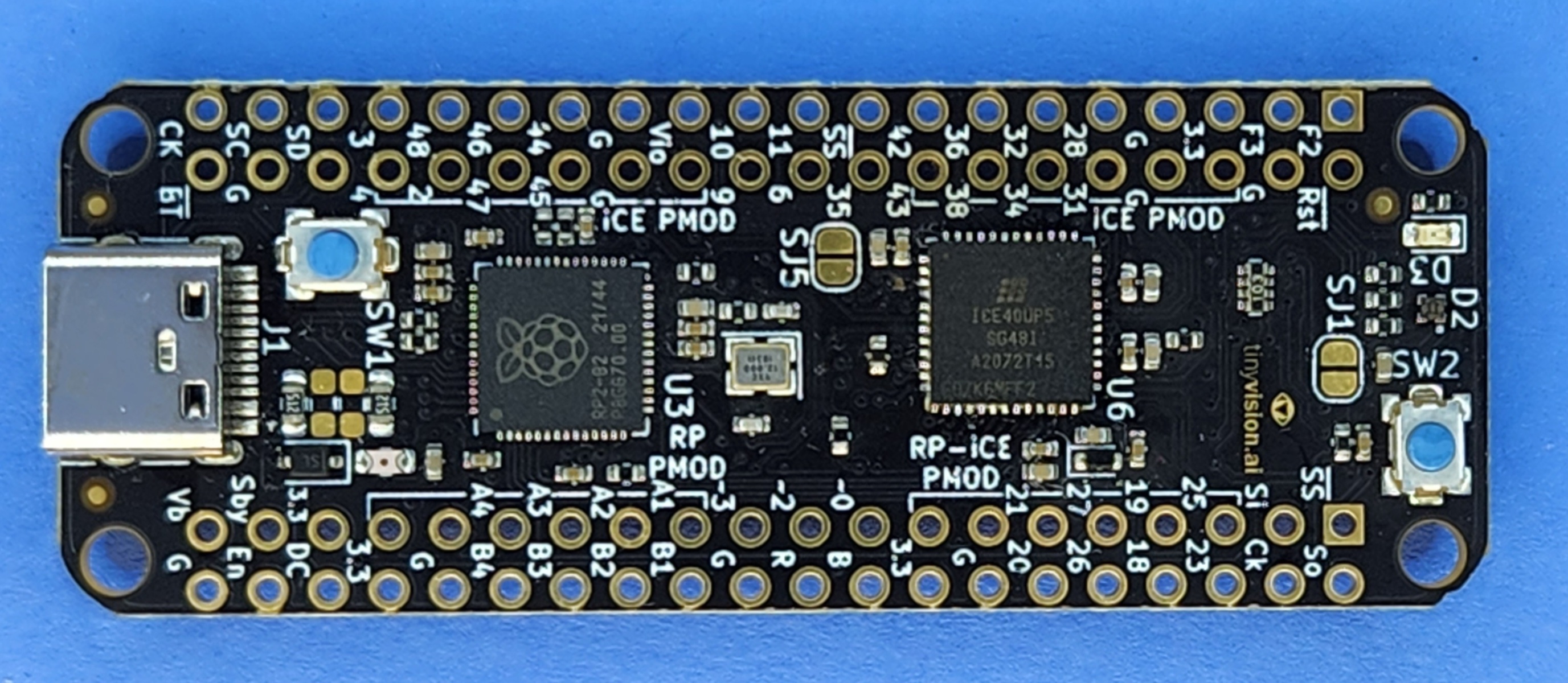
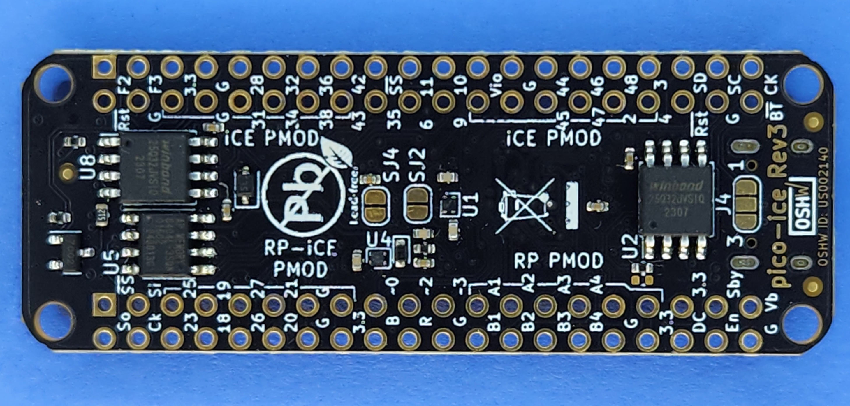
The pico-ice is a small, low cost board with the Raspberry Pi Pico processor (RP2040) and a Lattice Semiconductor iCE40UP5K FPGA. The board features independent flash for the FPGA and RP2040, low power SSRAM, a couple of pushbuttons and a 3 color LED with all FPGA and RP2040 pins brought out to easy to use 0.1" header pins (arranged as PMOD's) for fast prototyping.
The tinyVision.ai pico-ice Board Features:
- RaspberryPi RP2040 processor
- Lattice UltraPlus ICE40UP5K FPGA with 5.3K LUTs, 1Mb SPRAM, 120Kb DPRAM, 8 Multipliers
- ALL RP2040 and 32 FPGA GPIO on 0.1” headers
- 4MB SPI Flash
- 8MB low power qSPI SRAM
- RGB LED, shared between the RP2040 and FPGA
- 2 pushbuttons, 1 dedicated and 1 primarily for processor reset during development but can be repurposed for user applications when not used for reset
- On board 3.3V and 1.2V Regulators, can supply 3.3V to your project
- Open source schematic and layout using KiCAD design tools
- 4 layer board with a solid ground plane for good signal integrity
- FPGA clock supplied by the RP2040, easy to program FPGA clock under SW control
- Examples for communicating to the FPGA over SPI
- Support for ultra low power sleeep mode: can shut down the RP2040 and FPGA while keeping the SRAM powered
Firmware features:
- pico-ice library to support drag-drop programming of the FPGA bitfile: no need of any dedicated programmer
- Alternate programming of the FPGA flash using DFU mode
- FPGA clock under RP2040 control
- Passthrough UART code enables transparent access to the FPGA's UART for debug/logging/control
OSHW US002140 | Certified open source hardware | oshwa.org/cert


