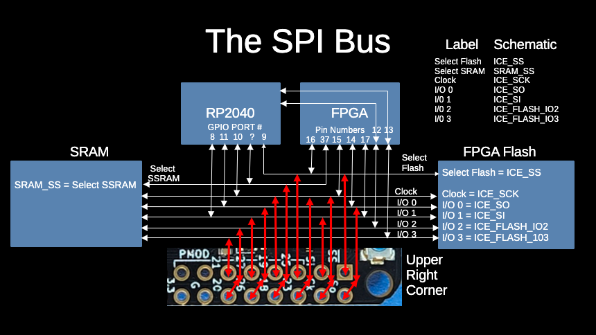
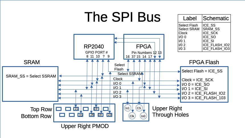
The RP2040 pins have been named.  All but the SRAM chip select.
    The mapping between board signals, and diagram labels has been added, both
    as a table, and in the FLASH and SRAM blocks.
    The titles and file names are changed to SPI Bus, and spi_bus_black.*
    or spi_bus_white.*
1.9 KiB
Pinout Diagram
This diagram shows the ICE40 and RP2040 names for the through holes on the pico-ice board.
With RTL on the iCE40
To program the FPGA, one needs to tell the synthesis tools which pins to connect to the signals in your RTL. There are two different ways to name the pins. The wafer names are words like IOB_6a and IOT_8b, and the pin numbers have names like ICE_2, ICE_3, and ICE_4.
Both sets of names can be found in this PCF file.
For Amaranth, until this gets upstreamed, the various board resources including its pins are defined on
pico_ice.py.
With code on the RP2040
The FPGA pins and other signals are defined in pico_ice.h.
The PMOD pins can also be accessed from
pmod.h and
ice_pmod.h.
SPI Pinouts
For debugging the FPGA <-> SPI <-> Flash/RAM interface it is very helpful to use the 4 through holes on the upper right of the FPGA, and to connect a logic analyzer to the upper right PMOD. These two diagrams may help. Remember that the default boot process leaves the Flash switched off. With the Yosys icepack command, the -s option boots the Flash in the on state.


